Skip to content
GaN Telecom Power: When a SiC Diode Is the Right Partner
Last Updated: 2026-10-13
Quick Answer
A GaN switch does not automatically require a separate SiC diode. In a conventional boost stage, SiC can reduce recovery-related turn-on stress; in an active totem-pole stage, controlled switches perform the main rectifying function. Identify the topology, then compare device charge, layout, thermal behavior and system efficiency.
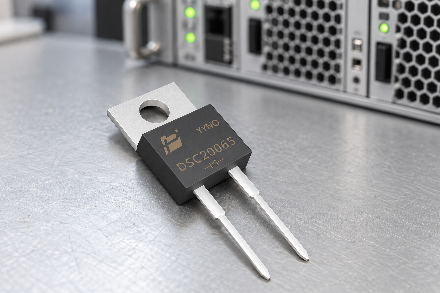
Product scene based on the supplied DSC20065 reference; application suitability is evaluated separately.
Let the Topology Define the Partnership
The circuit determines whether a discrete boost diode is present. A conventional boost PFC stage has a diode that commutates against the switching device. In an active totem-pole architecture, switches assume the principal rectifying roles, so a discrete SiC boost diode is not universally required.
TI’s TIDA-010203 GaN totem-pole PFC design provides a concrete active-stage example. A telecom power shelf may also include isolated DC/DC conversion, output protection and auxiliary supplies. Map those stages separately instead of calling every semiconductor next to a GaN switch its necessary diode partner.
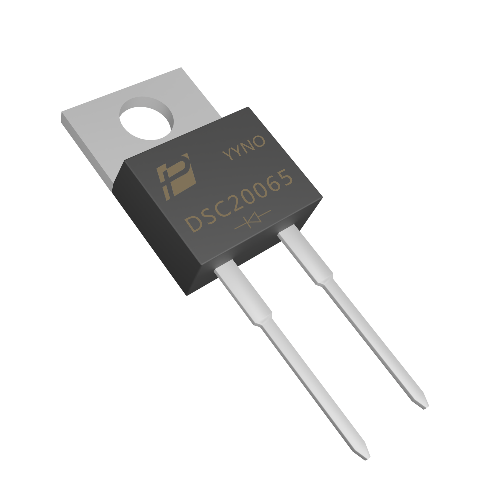
Supplied DSC20065 product reference; no system-level suitability or qualification is implied.
Evaluate a SiC Candidate Only Where a Diode Is Needed
POWERSi DSC20065 is a 650 V SiC Schottky device in a two-lead TO-220AC package, identified by the supplied V2 documentation and matching product image. It illustrates the kind of discrete candidate that could be assessed for a suitable diode position. The image does not imply that the device is installed in a specific telecom rack.
Check the circuit’s reverse-voltage stress, current waveform, mounting constraints and cooling budget before considering the part. The headline voltage class is not a substitute for transient margin. Likewise, the choice of GaN for a neighboring switch does not establish the diode’s package, current rating or thermal suitability.

Fast switching makes parasitics important.
Account for Charge and the Commutation Loop
A SiC Schottky diode avoids silicon PN minority-carrier recovery, but its capacitance still moves charge during a voltage transition. Compare the candidate’s relevant charge and forward-loss behavior under the intended operating conditions. Do not interpret a zero-recovery marketing phrase as zero switching energy throughout the circuit.
| Check | What to observe |
|---|---|
| Commutation current | Switch turn-on peak and diode charging current |
| Voltage stress | Overshoot and ringing at relevant load and temperature |
| Layout | Power-loop inductance and coupling into control paths |
| Measurement | Probe bandwidth and connection-induced ringing |
Keep gate drive, layout and probing consistent for the initial comparison. If one of those changes, record it as part of the evaluated configuration.

Illustrative application scene; not a customer installation or a measurement result.
Measure the Power Shelf Across Its Duty Cycle
A base-station power system does not necessarily operate at a single fixed load. Evaluate the load points and module-sharing strategy relevant to the installation, including standby or reduced-load operation where applicable. A component improvement at rated load may contribute little during the states where the system spends most of its time.
Measure whole-module input and output power with suitable instruments and repeatable thermal conditions. Keep losses in magnetics, switches, rectifiers and cooling separate in the analysis. A product photograph or topology label cannot establish a particular efficiency gain, energy saving or improvement in field reliability.

Define the engineering scope first.
Choose Between a Component Change and a Topology Change
Replacing a silicon boost diode with SiC and redesigning a bridge stage as a GaN totem pole are different projects. The latter changes control, protection and commutation paths as well as components. Do not attribute the benefit of a whole architecture change to one diode substitution.
Provide POWERSi with the specific diode position, original code, switching waveform and installed cooling requirements when evaluating a discrete option. Establish acceptance limits for stress, efficiency, temperature and emissions. Choose the combination that meets those limits in the actual telecom module, rather than assuming GaN and SiC must always appear together.
Key Takeaways
- GaN does not dictate one diode choice.
- Fast switching makes parasitics important.
- Define the engineering scope first.
Conclusion
Start with the telecom module topology and the measured commutation problem. Contact POWERSi with that operating envelope to discuss a suitable discrete diode option.
FAQs
Does every GaN power stage require a SiC diode?
No. The topology determines whether a discrete rectifying diode is needed.
Where can SiC be helpful alongside GaN?
A suitable hard-switched diode position may benefit from reduced minority-carrier recovery stress.
Does SiC remove capacitive switching current?
No. Device capacitance still charges and discharges.
Does a diode upgrade equal a totem-pole redesign?
No. A topology change also changes current paths, control and protection.
Can peak efficiency alone predict site energy savings?
No. The load profile, module operation and complete system losses also matter.