Skip to content
SiC and FRED Alternatives in PV Inverters: Validate the Operating Envelope
Last Updated: 2026-10-08
Quick Answer
PV inverter diode alternatives must be evaluated at a defined circuit position across the operating envelope. A boost rectifier, inverter freewheel path and auxiliary supply rectifier do not face identical stresses. Compare commutation, blocking, conduction and thermal behavior under relevant operating conditions, then assess system performance without assuming a universal SiC or FRED advantage.
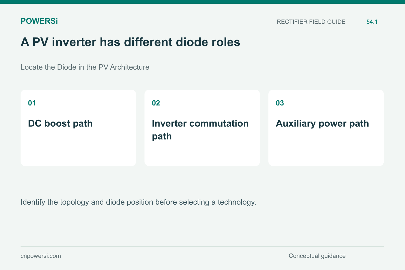
A PV inverter has different diode roles.
Locate the Diode in the PV Architecture
Identify the topology and diode position before selecting a technology. A DC boost diode can experience hard commutation; another path may have different switching conditions or be integrated into a power module. An auxiliary supply is a separate design problem.
Infineon’s SiC application overview includes solar power conversion, but an application category does not approve a particular alternate. Map the actual semiconductor functions and distinguish discrete candidates from changes to an integrated switching assembly.
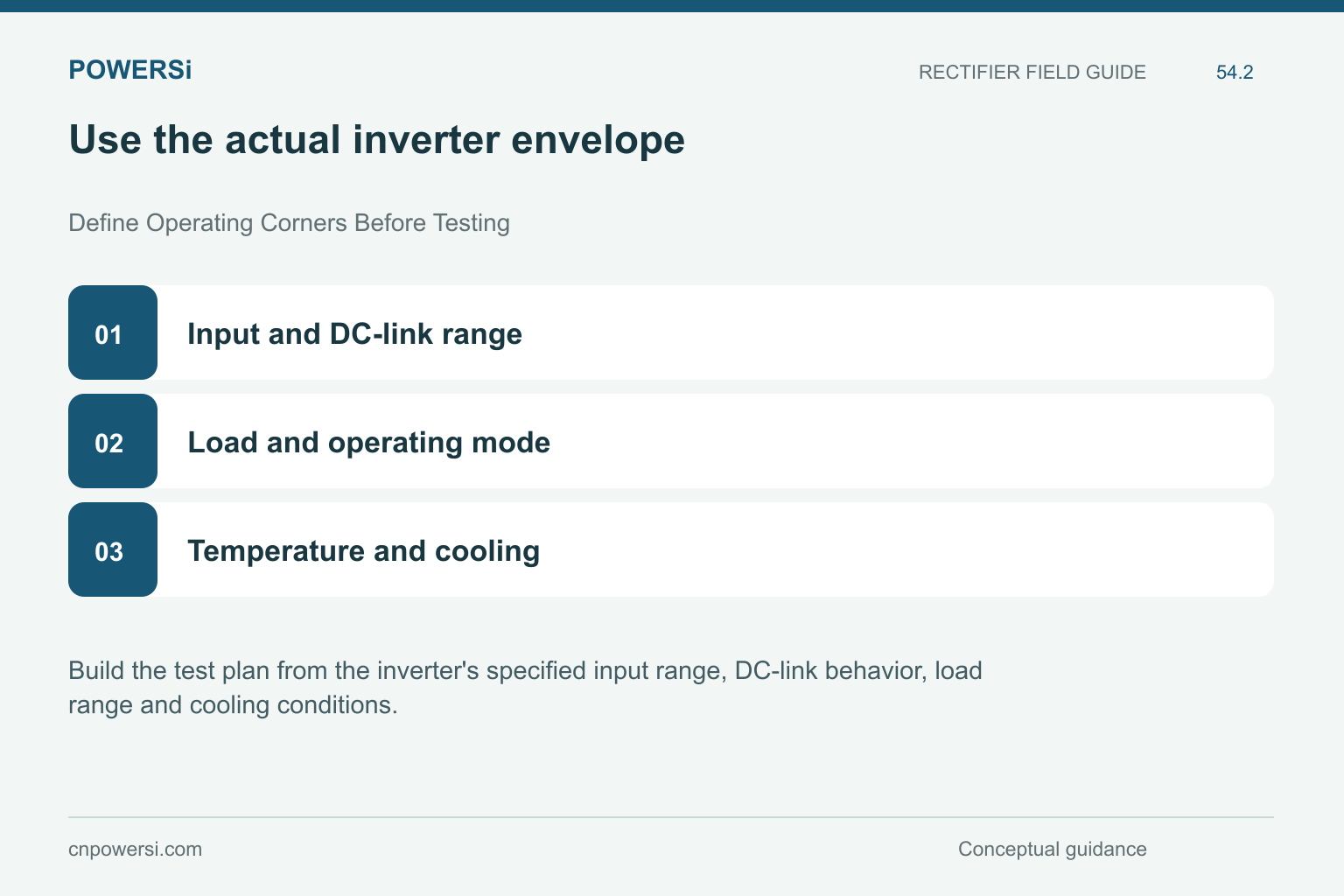
Use the actual inverter envelope.
Define Operating Corners Before Testing
Build the test plan from the inverter’s specified input range, DC-link behavior, load range and cooling conditions. Include relevant startup, shutdown and control transitions. Voltage stress depends on the actual circuit and overshoot, not only the nominal PV voltage.
Avoid selecting only the operating point where a candidate performs best. A change that reduces loss at rated load can behave differently at light load or a different input condition. Keep the acceptance criteria tied to the system requirements at each relevant corner.
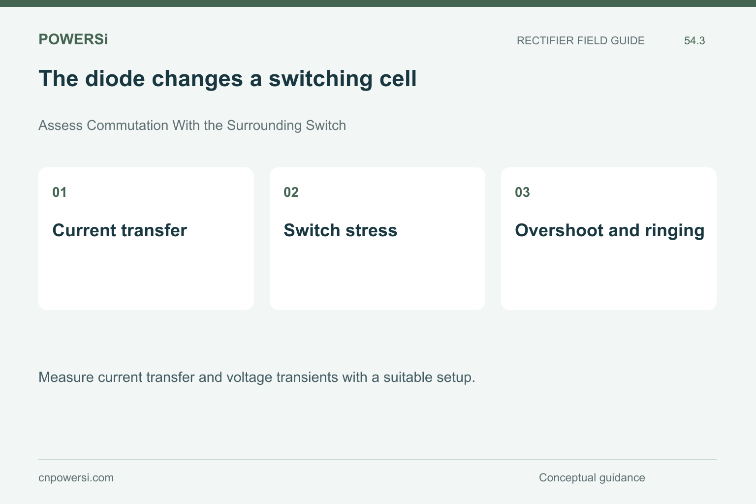
The diode changes a switching cell.
Assess Commutation With the Surrounding Switch
Measure current transfer and voltage transients with a suitable setup. Evaluate the interacting switch and layout, since changing a diode can alter switching stress and ringing elsewhere in the cell. Compare the same operating points and measurement method.
For SiC Schottky candidates, include capacitive effects rather than assume no dynamic current. For silicon fast-recovery candidates, preserve the recovery test conditions and waveform context. Neither a single recovery-time number nor a technology label establishes the full converter result.
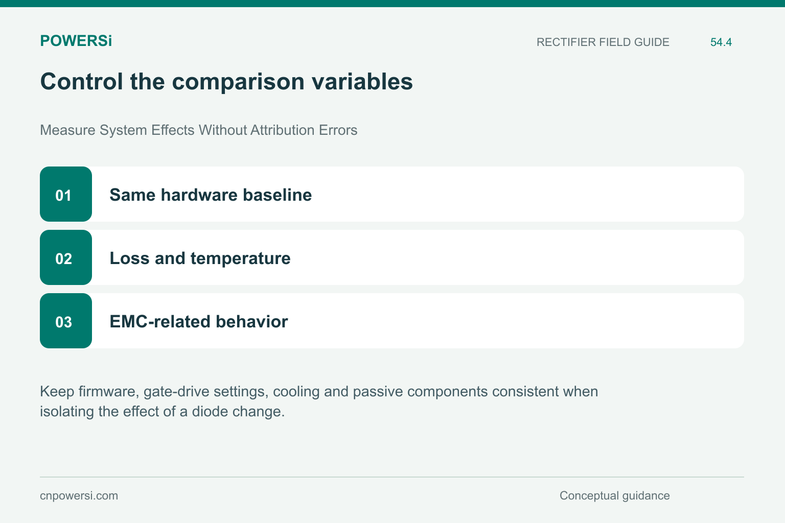
Control the comparison variables.
Measure System Effects Without Attribution Errors
Keep firmware, gate-drive settings, cooling and passive components consistent when isolating the effect of a diode change. If a redesign is needed, document those changes and distinguish the combined result from the diode-only comparison.
Measure loss or efficiency with sufficient accuracy for the claimed difference and check temperature at relevant locations. Observe conducted or radiated disturbance behavior using an appropriate system test plan. A reduction in one switching loss term is not automatically the same percentage improvement in total inverter efficiency.
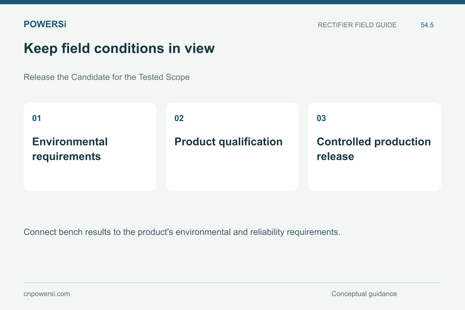
Keep field conditions in view.
Release the Candidate for the Tested Scope
Connect bench results to the product’s environmental and reliability requirements. Consider the intended thermal exposure, assembly and operating profile; do not convert a short bench run into a field-lifetime claim.
The final release should identify the exact diode, board configuration and permitted operating envelope. This article describes an evaluation method, not a measured POWERSi inverter installation. Request application-specific evidence before making efficiency, lifetime or direct-replacement claims for any candidate.
Key Takeaways
- A PV inverter has different diode roles.
- The diode changes a switching cell.
- Keep field conditions in view.
Conclusion
Start the inquiry with topology, diode position and operating envelope. Share those requirements with POWERSi to identify candidates for a controlled PV evaluation.
FAQs
Does every PV inverter need the same diode?
No. Architecture and circuit position determine the required function and stress.
Can a rated-load test cover the whole envelope?
No. Relevant input, load, control and thermal corners also need assessment.
Does lower diode switching loss equal the same inverter efficiency gain?
No. Total system loss includes other devices and operating effects.
Should gate-drive changes be documented?
Yes. They can affect whether the measured result is attributable to the diode alone.
Is this a report of a tested POWERSi installation?
No. It is an application validation framework, without invented field results.