Skip to content
Rectifier Selection by Topology: Buck, Boost, Flyback and Bridge Circuits
Last Updated: 2026-10-07
Quick Answer
Rectifier selection by topology starts with the current path in each switching state. Determine when the diode conducts, what reverse voltage it blocks and how its current ends. Those conditions define the required voltage, current, dynamic behavior and cooling. A converter’s output voltage or switching frequency alone cannot identify the right rectifier.
The same nominal output can be produced by different circuits with different diode stresses. Even within one topology, continuous and discontinuous conduction can change commutation. Draw the relevant current paths before choosing a technology or copying a part from another design.
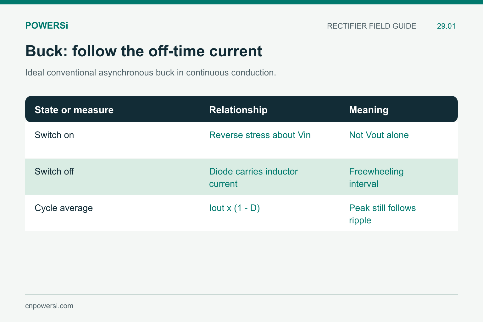
Ideal conventional asynchronous buck in continuous conduction.
Asynchronous Buck: Follow the Freewheeling Interval
In the conventional positive-output asynchronous buck, the catch diode conducts inductor current while the high-side switch is off. While the switch is on, the diode blocks approximately the input voltage in the ideal circuit. Its reverse stress is therefore not simply the lower output voltage.
For ideal continuous conduction, duty ratio D is approximately Vout/Vin. The diode’s cycle-average current is approximately Iout × (1 − D), while its peak follows the inductor-current peak. For an ideal 48 V to 12 V, 4 A example, D = 0.25 and diode average current is about 3 A. This calculation omits losses and ripple effects; it does not by itself approve a 3 A device.
At switch turn-on in continuous conduction, the diode is forced out of conduction. Recovery or capacitive charge, switch turn-on loss and overshoot then become part of the comparison. A synchronous buck uses a controlled switch in this position and requires a different device-and-drive assessment.
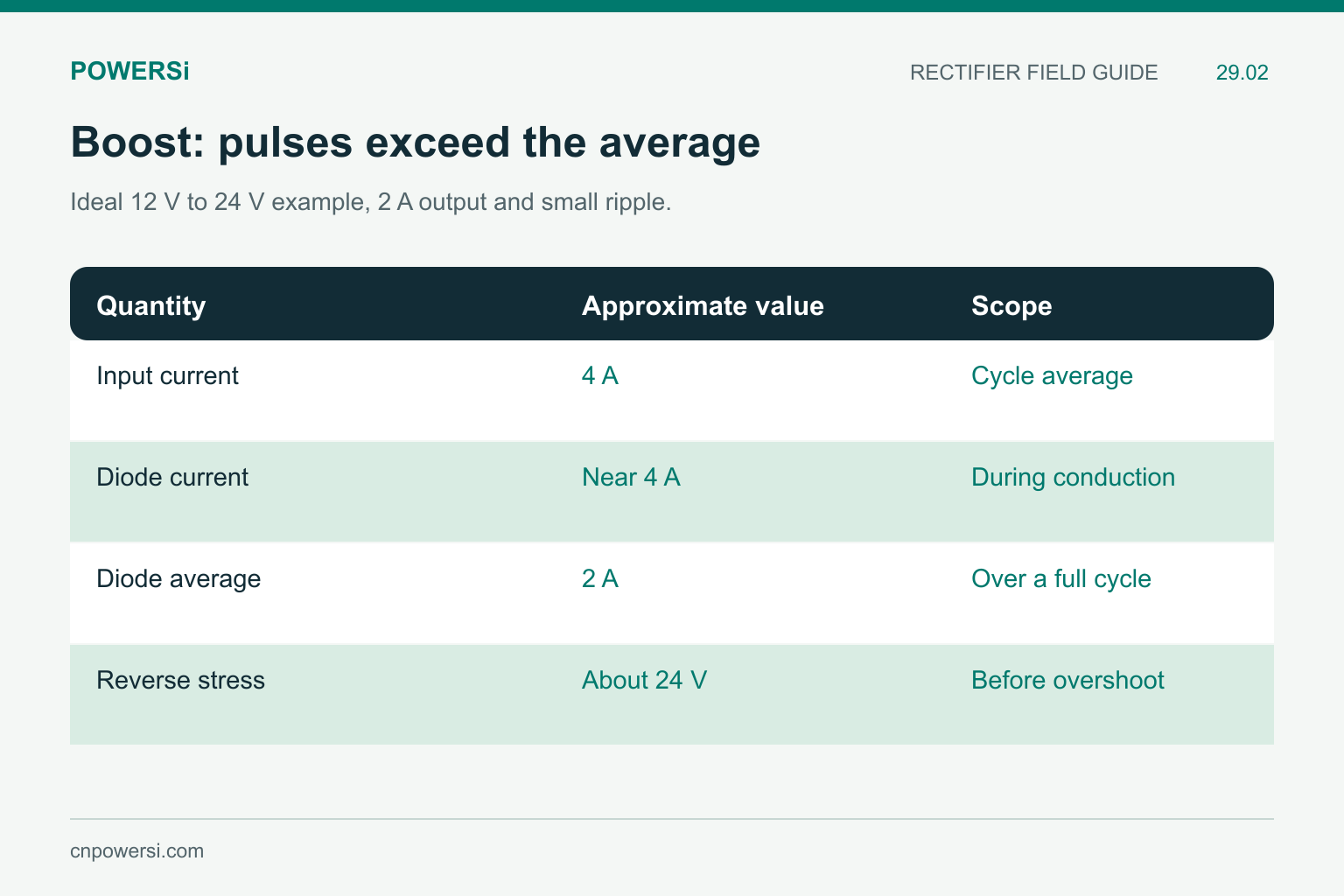
Ideal 12 V to 24 V example, 2 A output and small ripple.
Boost: Separate Average Current From Pulse Current
In a conventional asynchronous boost converter, the output diode conducts when the main switch turns off. When the switch is on, the diode blocks approximately the output voltage in the ideal circuit. Check output tolerance and switching overshoot rather than choosing the diode from input voltage alone.
In steady state, the diode’s average current over a complete cycle equals output load current because the output capacitor has zero net charge change. During conduction, however, the diode carries inductor current, which can be substantially higher than output current. Peak and RMS current still require the actual waveform.
For an ideal 12 V to 24 V boost with a 2 A output, average input current is 4 A. At roughly 50% duty and small ripple, diode current is near 4 A during its conducting interval even though its cycle average is 2 A. Real losses and ripple alter the values.
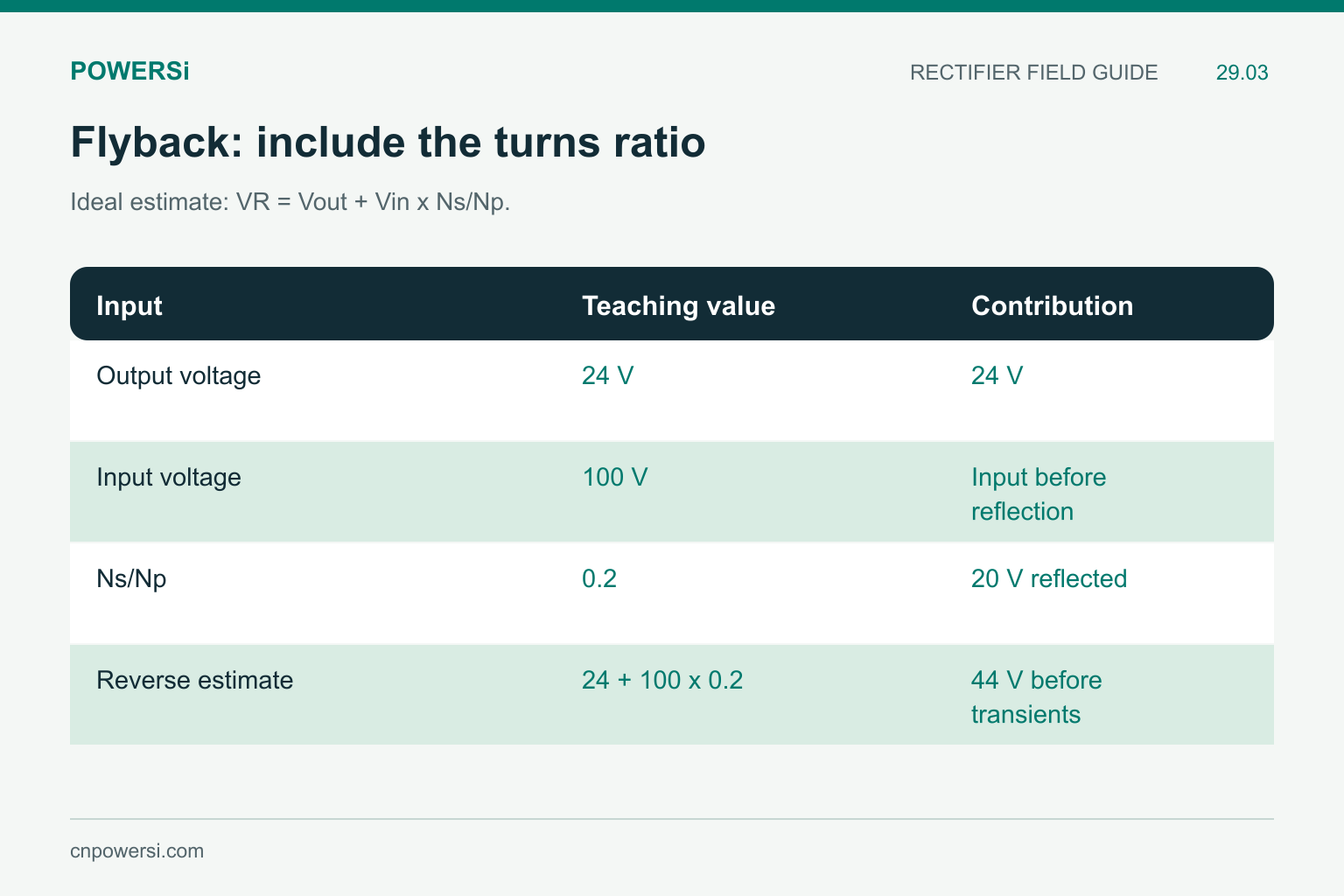
Ideal estimate: VR = Vout + Vin x Ns/Np.
Flyback: Include the Reflected Input Voltage
In a conventional isolated flyback, the secondary diode conducts during the energy-transfer interval after the primary switch turns off. During primary on-time it blocks the output voltage plus the input voltage reflected to the secondary. TI’s flyback application brief illustrates these operating states and current waveforms.
Ignoring parasitic transients, a useful first estimate is VR = Vout + Vin × Ns/Np, where Ns/Np is secondary turns divided by primary turns. With hypothetical values of 24 V output, 100 V input and Ns/Np = 0.2, this gives 44 V before tolerances and overshoot. Reversing the turns-ratio definition would produce the wrong result.
In discontinuous conduction, secondary current reaches zero before the next primary turn-on. In continuous conduction, it remains nonzero until commutation. That difference changes the switching assessment, but does not remove capacitance, ringing or voltage-margin requirements in discontinuous operation.
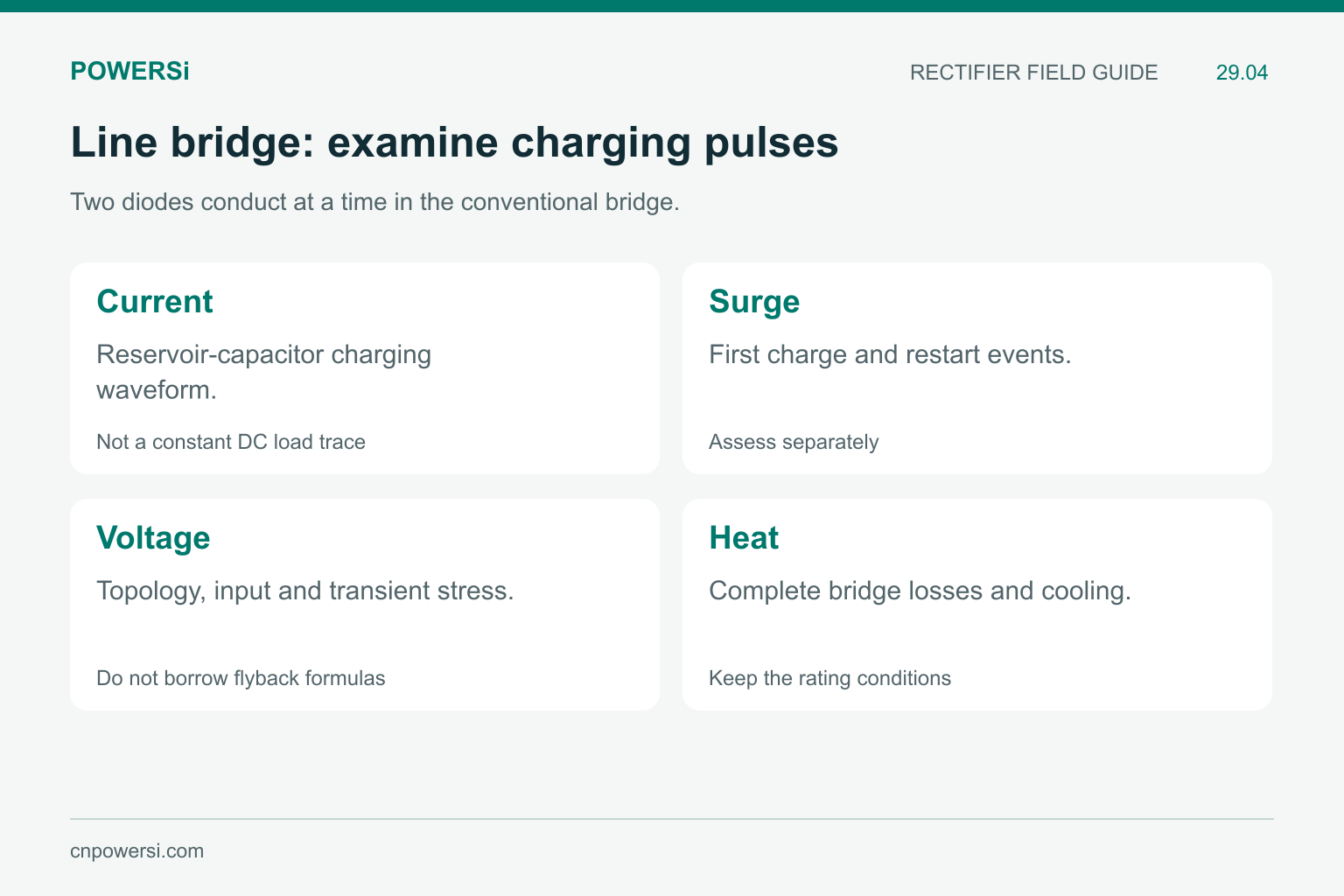
Two diodes conduct at a time in the conventional bridge.
Line Bridge: Include the Reservoir Capacitor
A conventional full-wave bridge conducts through two diodes at a time. With a reservoir capacitor, conduction occurs in charging pulses rather than a constant current equal to the DC load. Evaluate the bridge’s complete current definition, charging waveform, startup surge and heat removal.
Do not apply the buck or flyback reverse-voltage expressions to a line bridge. Likewise, the converter’s downstream switching frequency does not make its line-input bridge a high-frequency output rectifier. Each diode position has its own operating waveform.
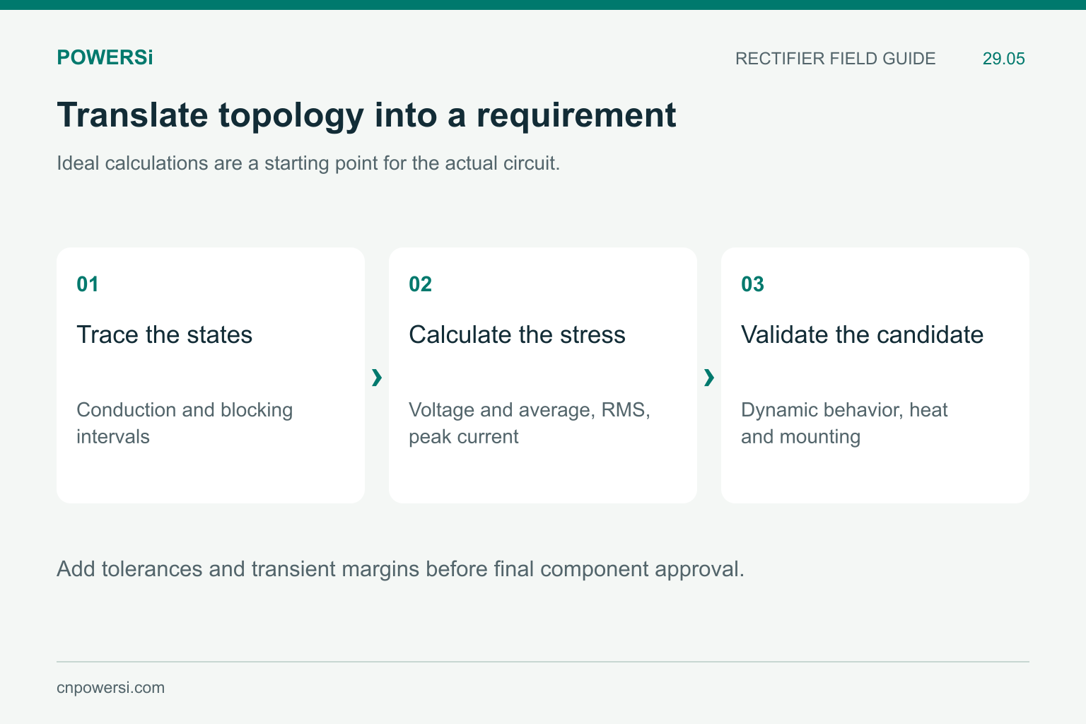
Add tolerances and transient margins before final component approval.
Turn the State Analysis Into a Candidate List
For each position, record maximum reverse stress, forward average/RMS/peak current, conduction duty and the event that ends conduction. Add hot losses, startup conditions and the available cooling. Only then compare silicon Schottky, recovery-diode or SiC candidates that fit the required voltage class.
The ideal formulas above establish starting estimates. Validate the actual assembly over input and load range, including abnormal conditions within the design’s scope. Keep the exact connection and package requirements alongside the electrical result; the right technology in the wrong terminal arrangement still cannot serve as an approved replacement.
Key Takeaways
- Buck catch-diode reverse stress follows input voltage in the ideal circuit.
- Boost diode average current does not describe its conducting pulse peak.
- Flyback reverse stress includes the secondary-reflected input voltage.
- Conduction mode and circuit position determine the dynamic assessment.
Conclusion
Topology turns a broad selection question into measurable stresses. Include the switching states, turns-ratio definition where relevant and current waveforms when discussing POWERSi rectifier candidates.
FAQs
Should a buck catch diode be rated from output voltage alone?
No. In the conventional ideal buck it blocks approximately the input voltage, before added stress allowances.
Does a 2 A boost output imply a 2 A diode peak?
No. The diode carries inductor-current pulses during its conducting interval.
Which turns ratio is used in the flyback example?
Ns/Np means secondary turns divided by primary turns.
Does discontinuous conduction eliminate every switching loss?
No. Capacitive effects, ringing and other losses remain even when diode current reaches zero before commutation.
Do the ideal examples select a final part rating?
No. Add tolerances, transient stress, thermal requirements and the applicable design margin.