Skip to content

Last Updated: November 5, 2026
Key Engineering Takeaways
- Check the PFC diode’s measured reverse-voltage peak, current waveform and thermal limits.
- Compare capacitive charge and forward voltage at matching test conditions.
- The DSC30120P public current fields differ; obtain a controlled clarification before qualification.
In hard-switched boost PFC, choose the SiC diode by evaluating its blocking-voltage margin, hot current capability, forward loss and capacitive commutation behavior in the same circuit. SiC Schottky technology can reduce the minority-carrier recovery associated with a silicon PN diode, but it still has capacitance, heat and switching-related energy. The final decision depends on measured system performance, not a single charge or current number.
What happens when the PFC switch turns on?
In a conventional boost stage, inductor current flows through the boost diode when the switch is off. When the switch turns on, it drives the diode toward reverse bias. With a silicon PN diode, stored minority charge produces reverse recovery current; a SiC Schottky diode avoids that same minority-carrier storage mechanism, but its nonlinear junction capacitance still must be charged and discharged. The resulting current affects the switch, diode, parasitic inductance and voltage ringing.
This analysis concerns a hard-switched boost PFC diode. It should not be applied unchanged to bridgeless, totem-pole or soft-switched circuits, where current paths and switching events differ. The existing hard-switching diode comparison addresses silicon FRED and ultrafast parts; this guide focuses on SiC charge and practical PFC measurement.
Build a comparable shortlist
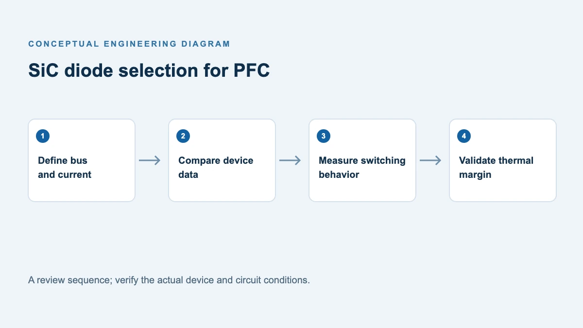
| Selection item | Match the actual circuit | Why it matters |
|---|---|---|
| Reverse blocking | DC bus maximum, overshoot, tolerance and transients against VRRM | Nominal bus voltage alone misses peak diode stress |
| Current and thermal | Waveform, average, RMS and peak current, case temperature and derating conditions | A headline current rating is a conditional thermal limit |
| Forward behavior | VF versus current and junction temperature, typical versus maximum | Conduction loss and diode heating may offset switching benefits |
| Capacitive charge and energy | Compare QC and EC at the same reverse voltage and temperature | Charge is voltage-dependent; it is not the entire converter switching loss |
| Surge and mechanics | Startup or fault pulses, package, tab connection, isolation and cooling | Electrical and physical compatibility are both necessary |
For the PFC bus, evaluate the maximum regulated and transient voltages, tolerances, layout-induced ringing and any applicable system requirements. A 1200 V part is not automatically necessary for every bus, nor is it automatically adequate in every topology. The selection depends on real maximum diode stress and design margin.
Current is equally conditional. Low-line full-load operation can produce a demanding input-current waveform; bus overvoltage, light load, startup and fault cases may stress different parameters. Estimate conduction loss from the actual diode-current waveform and VF curve across the line and switching cycles. Add switching-related loss using an appropriate model or measured energy. Verify the sink and interface at the worst local ambient.
Read DSC30120P numbers with their conditions
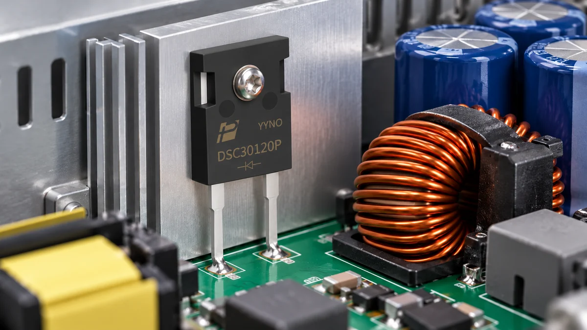
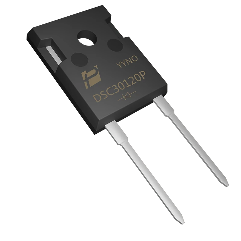
The POWERSi DSC30120P is listed as a single 1200 V SiC diode in TO-247AC, with 30 A specified at a 140 °C case temperature. The product page reports typical capacitive charge of 155 nC at 800 V and 25 °C; that is a typical point, not a maximum guarantee, and it cannot by itself determine the loss at another voltage or temperature.
The same page lists VF at 30 A as 1.45 V typical and 1.59 V maximum at 25 °C, versus 2.11 V typical and 2.51 V maximum at 175 °C. These figures illustrate why current, temperature and typical/maximum designation must travel with a VF value. They are not a prediction of the device’s VF at a different current or of converter efficiency. The page also shows a separate “Rated IF” field of 15 A without an explanatory condition, while its detailed table and linked PDF state 30 A at Tc = 140 °C. Request a controlled datasheet and written clarification of that field before qualification.
The exposed metal tab is electrically connected to the cathode. If the sink must be held at another potential, select a suitable insulating interface and include its thermal resistance, creepage and clearance in the system design. Package appearance alone does not establish pin or tab compatibility.
Measure the switching cell, not just the diode
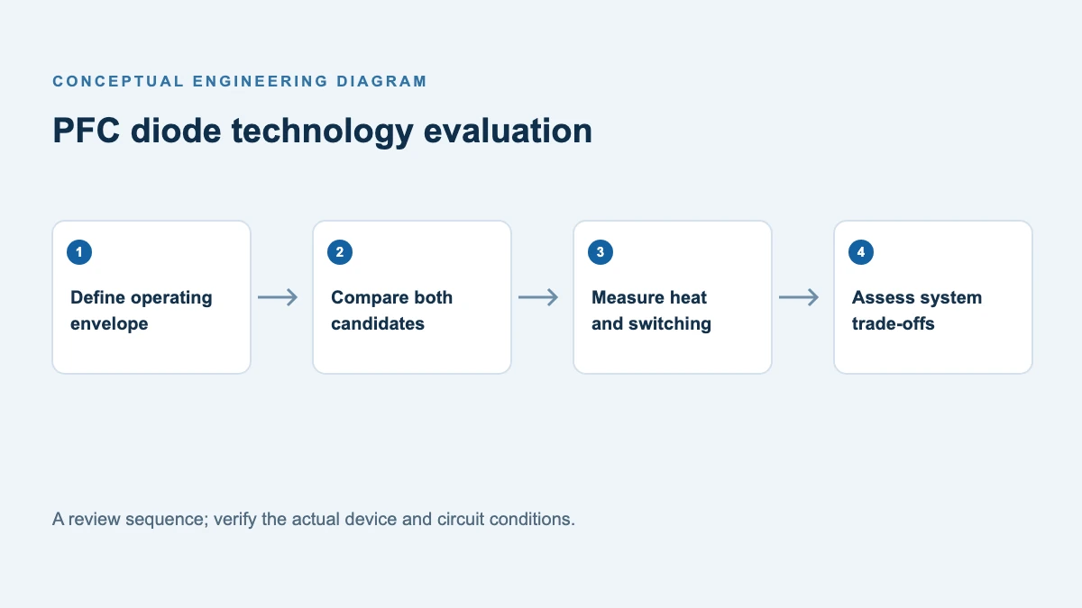
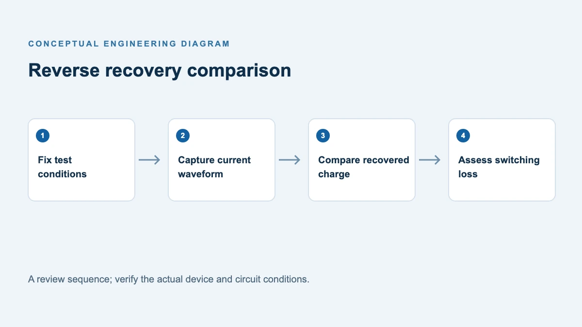
- Fix the comparison conditions. Use the same board, inductor, switch, gate drive, bus voltage, line condition, load, cooling and measurement setup. Identify any mechanical change that alters parasitics.
- Capture voltage and current together. Measure the diode reverse-voltage overshoot and commutation waveform, and the switch voltage/current at turn-on. Use properly rated, calibrated differential and current probes with short connections; account for probe loading, bandwidth, timing skew and measurement uncertainty.
- Compare energy at the event and total power. Integrate the synchronized switch voltage and current over a defined turn-on interval when appropriate. Measure input and output power over the same operating points. A lower recovery-related current does not guarantee an equal improvement in overall efficiency because forward loss, capacitance, control and other components also matter.
- Check heat and EMI in the finished assembly. After thermal stabilization, compare diode case, switch and heat-sink temperatures at worst local ambient. Assess ringing and conducted/radiated emissions using the actual layout and the required equipment test procedure. A cleaner-looking waveform alone is not compliance evidence.
Vishay’s PFC application note discusses why PFC diode selection must include switching as well as conduction and thermal capability. Use it for the method, not as performance data for POWERSi devices. The Power Integrations PFC design note likewise recommends evaluating diode choice against measured system efficiency.
What to send with an inquiry
Provide topology and conduction mode, line and bus range, switching frequency, peak/average/RMS diode currents, measured voltage overshoot, target efficiency, operating temperature, heat sink and isolation needs, and the existing part number. Include the test point and conditions when requesting help comparing charge and forward loss. Review the DSC30120P SiC rectifier details and contact POWERSi with the stated requirements. Request the controlled datasheet and written clarification of the 15 A and 30 A current fields; qualification remains an application-level test.
FAQ
Does a SiC Schottky diode have zero switching loss?
No. It avoids minority-carrier recovery typical of a silicon PN diode, but capacitive charge and other switching-cell losses remain. Total converter loss must be evaluated in context.
Is the highest current rating always the best diode?
No. A larger device may have different capacitance, forward loss, package or cost. Compare the actual operating waveform, thermal path and measured converter performance.
Can I compare two QC values measured at different voltages?
Not directly. Capacitance and charge depend on voltage. Compare like conditions or use each manufacturer’s curves and an appropriate energy model.
Does the exposed tab need electrical insulation?
It depends on the system. DSC30120P’s tab is connected to its cathode; verify the required sink potential and use an appropriate interface where isolation is needed.