Skip to content
Diode Reverse Voltage Margin: Why the Three-Times Rule Is Not Enough
Last Updated: 2026-09-30
Quick Answer
Diode reverse voltage margin should be based on the largest reverse stress across the actual device, including input tolerance and transients. A three-times multiplier is only a possible design heuristic, not a universal protection rule. Identify the waveform and failure mechanism, then apply the relevant rating, derating policy and protection strategy.
A failed diode does not prove that its voltage rating was too low. Excessive junction temperature, forward surge, assembly damage or incorrect polarity can also produce a short circuit. Replacing it with a higher-voltage part before investigating the operating conditions may leave the original cause in place.
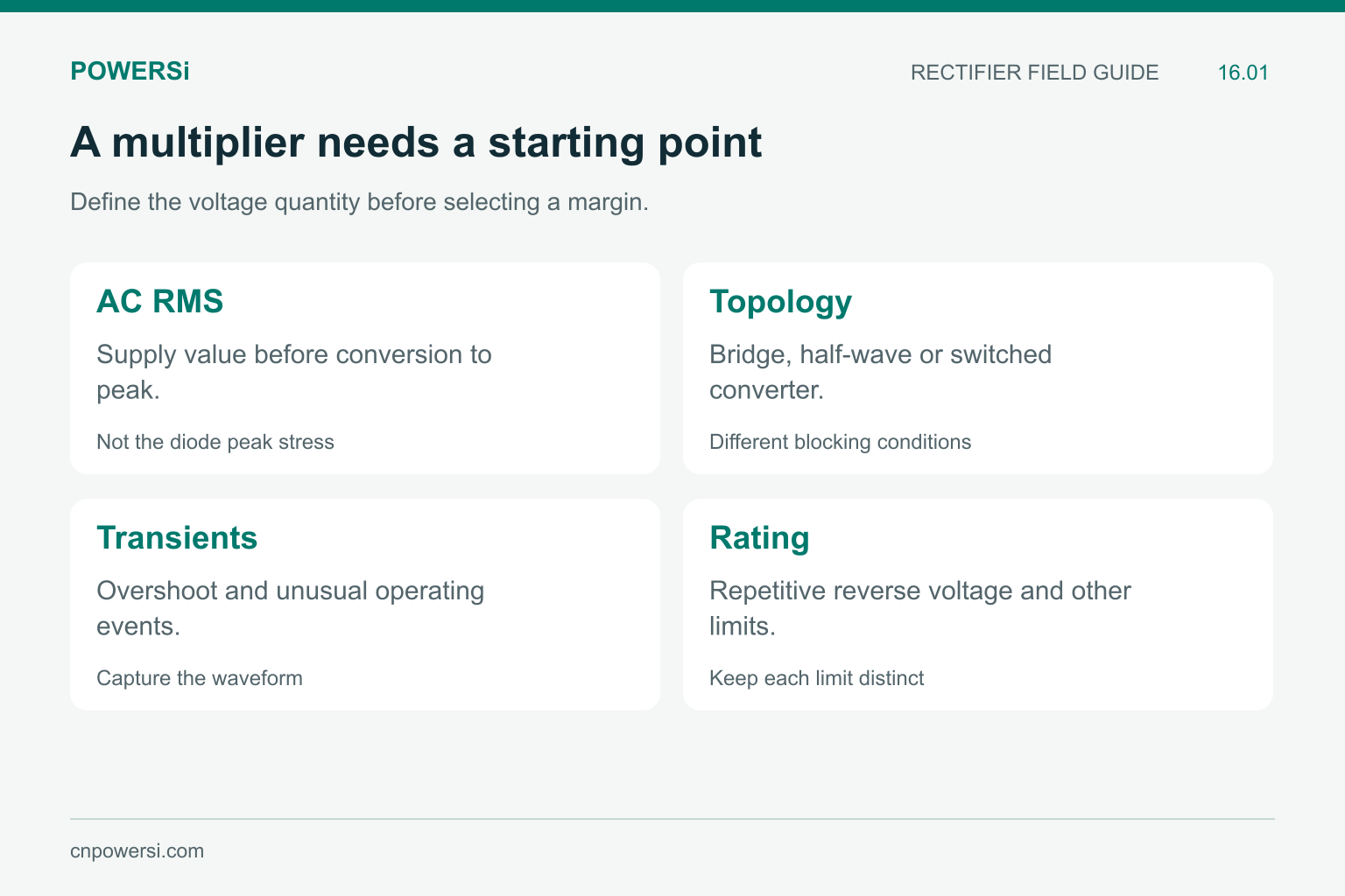
Define the voltage quantity before selecting a margin.
Define What the Multiplier Applies To
“Three times the voltage” is ambiguous. The starting value might be AC RMS input, DC output, transformer-secondary peak or a measured reverse-voltage maximum. These quantities can differ substantially. A multiplier cannot correct a mistaken starting quantity.
For a sinusoidal source, peak voltage is sqrt(2) times RMS voltage. In an ideal half-wave rectifier with a reservoir capacitor charged near the positive peak, the blocked diode can see approximately twice that source peak during the negative half-cycle. A conventional full bridge has a different blocking relationship. Neither expression should be transferred to an unrelated converter topology.
For example, an ideal 24 V RMS half-wave capacitor-input circuit can approach 67.9 V reverse stress before tolerances and transients: 2 × sqrt(2) × 24. Three times the nominal RMS value is 72 V, leaving little room above that ideal stress. This is a teaching example, not a recommended rating or a universal half-wave design margin.
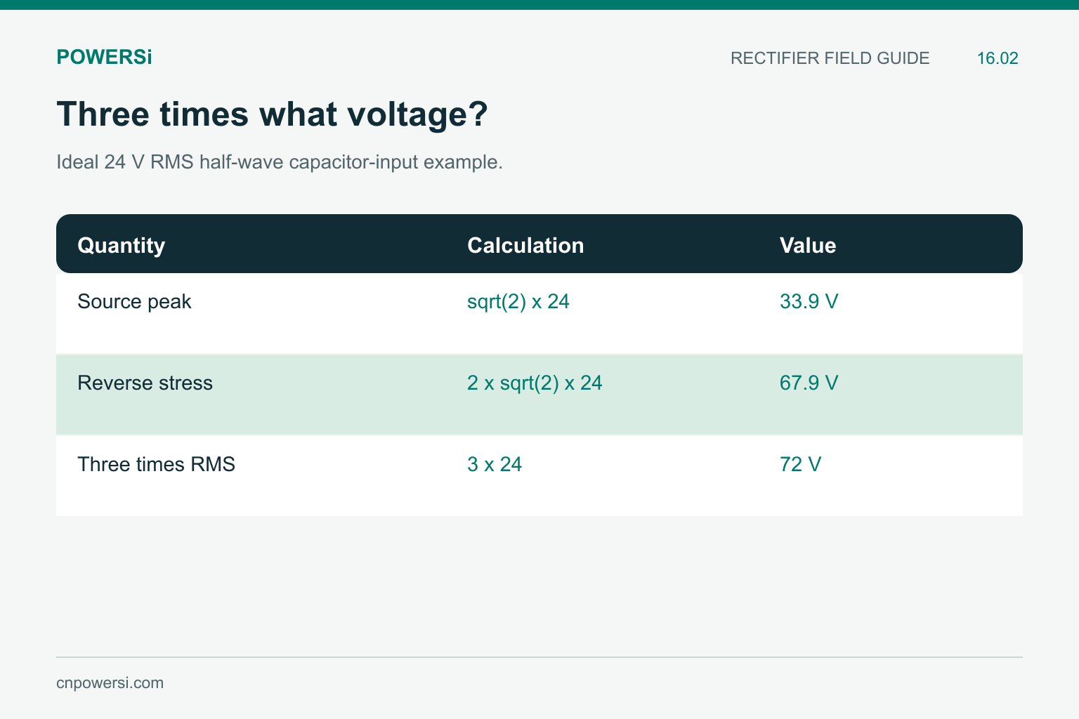
Ideal 24 V RMS half-wave capacitor-input example.
Establish the Worst-Case Waveform
Consider maximum input voltage, transformer regulation where applicable, no-load behavior, startup, shutdown and load changes. In switched circuits, parasitic inductance and commutation can add overshoot. Record both the repetitive waveform and unusual events rather than saving only one peak number.
Measure across the diode with appropriately rated equipment and a setup that controls probe-loop artifacts. A spike caused by the measurement loop is not a circuit stress, but an under-resolved real spike is not harmless either. Document probe placement, bandwidth, operating state and temperature so that the result can be reproduced.
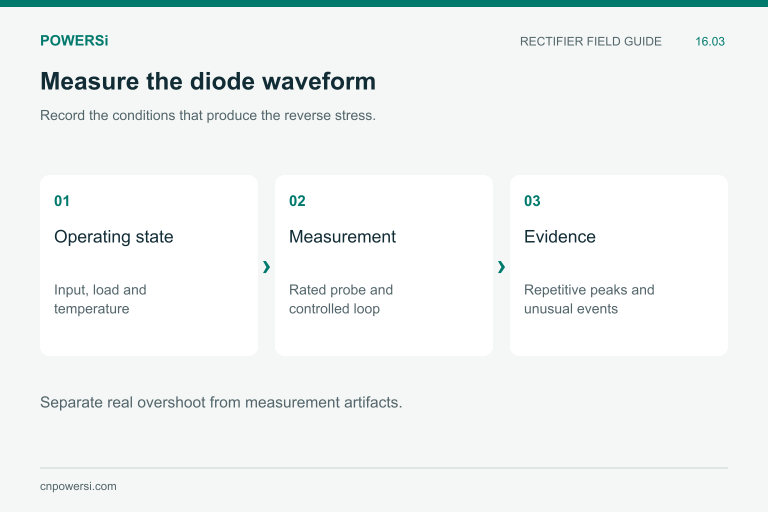
Separate real overshoot from measurement artifacts.
Compare the Correct Rating
VRRM is a repetitive peak reverse-voltage rating. It is not the same quantity as an AC RMS system voltage or a guaranteed avalanche-energy allowance. Do not assume that operation beyond VRRM is acceptable because the event is brief. Any permitted avalanche or non-repetitive behavior needs its own explicit specification and conditions.
Use the project’s derating requirement on the defined worst-case stress. If a hypothetical policy limits repetitive utilization to 80%, a 120 V design stress requires a rating of at least 150 V before any additional requirements are considered. The 80% value is an example policy, not a POWERSi rule or universal standard.
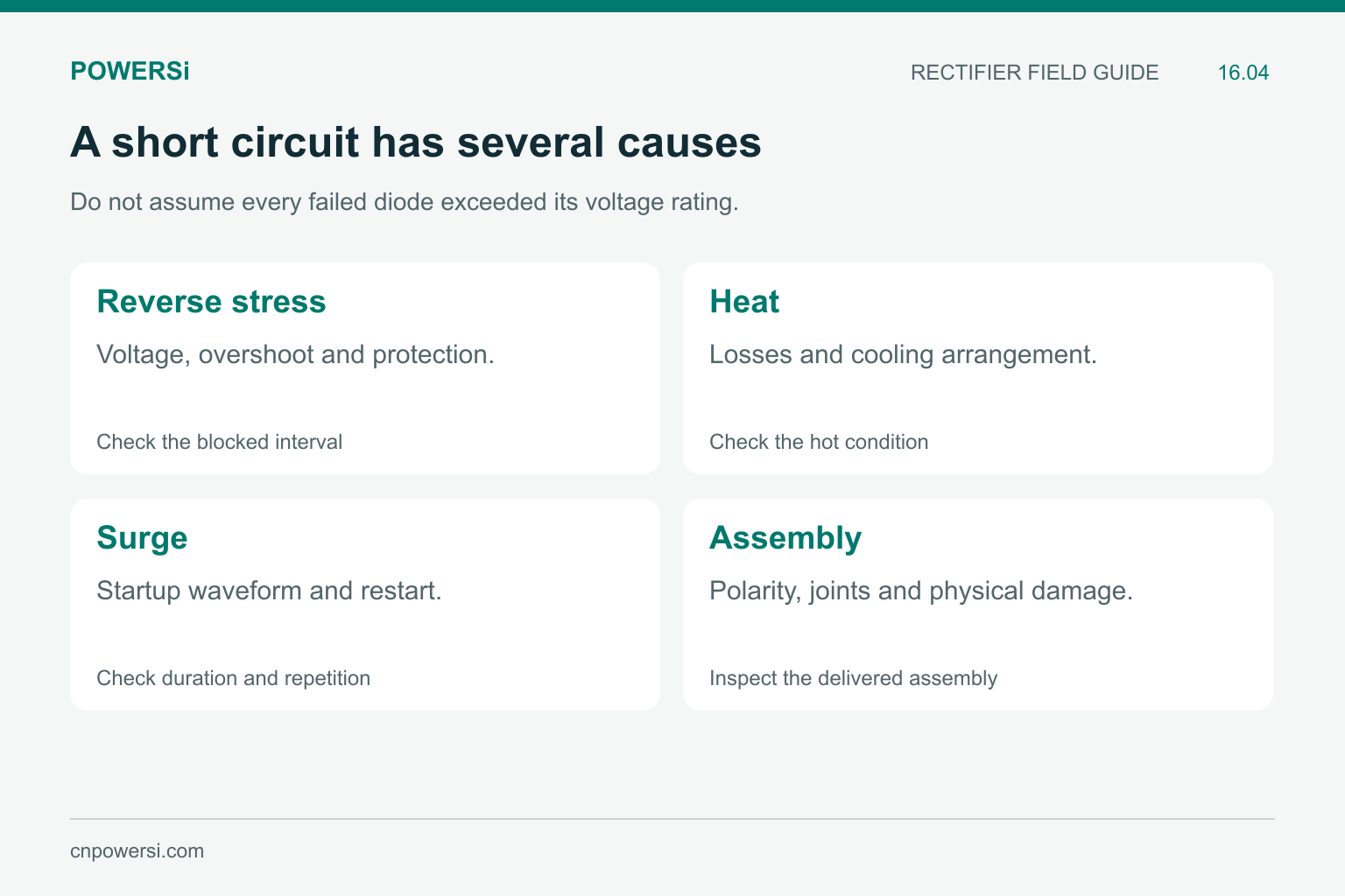
Do not assume every failed diode exceeded its voltage rating.
Diagnose Before Increasing the Rating
Inspect the failure sequence. Did the device become hot under steady load, fail at connection, or fail during switching? Compare the damaged location, assembly records and electrical measurements. Check surge current, cooling, reverse leakage, contamination and terminal orientation as well as voltage.
A replacement with higher VRRM may have different forward loss, recovery or leakage. Verify those differences rather than assuming that a larger voltage number is a complete upgrade. Protection can involve reducing loop inductance, controlling commutation or adding an appropriately designed clamp; each change needs circuit-specific assessment.
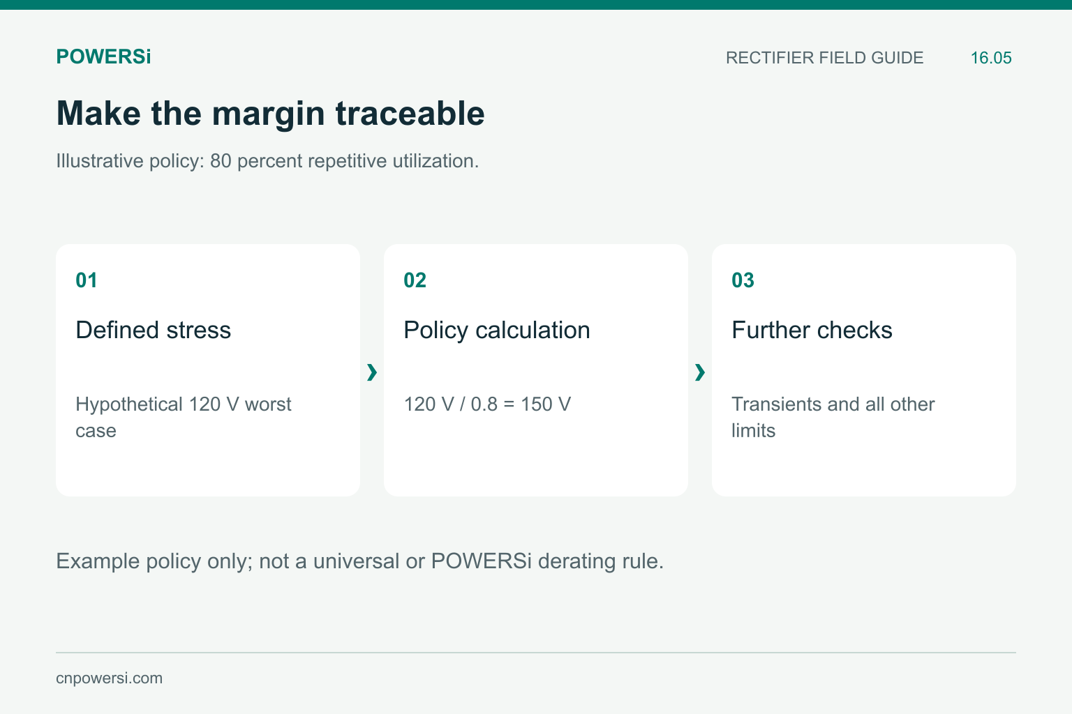
Example policy only; not a universal or POWERSi derating rule.
Release an Evidence-Based Margin
Keep the maximum observed or bounded reverse stress, applicable tolerance assumptions, selected voltage rating and utilization target together. Record how transient protection behaves and which operating conditions were evaluated. This gives a future buyer or engineer a reasoned replacement criterion rather than an unexplained multiplier.
Key Takeaways
- Define the voltage quantity before applying a margin.
- Topology determines the starting reverse stress.
- VRRM does not automatically permit avalanche operation.
- Investigate heat, surge and assembly causes alongside reverse voltage.
Conclusion
The useful margin is the one tied to a complete stress assessment. When discussing POWERSi rectifier options, provide the diode’s circuit position, worst-case waveform and operating temperature rather than only the nominal supply voltage.
FAQs
Is three times the supply voltage always sufficient?
No. The result depends on which voltage is multiplied, the topology, tolerances and transient conditions.
Does VRRM describe an RMS input voltage?
No. It specifies a repetitive peak reverse-voltage limit for the diode.
Can I ignore a short spike above VRRM?
No. A short duration does not establish permission to exceed a repetitive rating or a guaranteed avalanche capability.
Does a shorted diode prove reverse breakdown?
No. Several electrical, thermal and assembly failure mechanisms can lead to a short circuit.
What should accompany a voltage-rating substitution?
Include stress measurements, margin assumptions, protection behavior and comparisons of forward, recovery and thermal characteristics.